Wire Sizing and Spacing
Abstract—As the VLSI feature size has already decreased
below
lithographic wavelength, the printability problem, due to strong
diffraction effects, poses a serious threat to the progress of VLSI
technology. A circuit layout with poor printability implies that
it is difficult to make the printed features on wafers follow designed
shapes without distortions. The development of resolution
enhancement techniques (RET) can alleviate the printability
problem but cannot reverse the trend of deterioration. Moreover,
over-usage of RET may dramatically increase photo-mask cost
and increase the cycle time for volume production. Thus, there
is a strong demand to consider the subwavelength printability
problem in circuit layout designs. However, layout printability optimization
should not degrade circuit timing performance. In this
paper, we introduce a wire sizing and spacing method to improve
wire printability with minimal adverse impact on interconnect
timing performance. A new printability model is proposed to
handle partially coherent illuminations. The complex printability
and timing optimization problem is solved in a two-phase approach.
The difficulty of the printability optimization due to its
multimodal nature is handled with a sensitivity-based heuristic.
A coupling aware timing driven continuous wire sizing algorithm
is also provided. Lithographic simulation results show that our
approach can improve the printability in term of edge placement
error (EPE) by 20%–40% without violating timing, wire width,
and spacing constraints.
Index Terms—Design for manufacturing (DFM), optical
proximity
correction (OPC), physical design, timing optimization,
VLSI.
I. INTRODUCTION
THE MINIMUM transistor feature size of VLSI in mass
production has decreased to 65 nm and will shrink to
45 nm soon [1]. This miniaturization will be realized by
photolithography with a 193- or 157-nm wavelength. When
lithography entered subwavelength regime, strong diffraction
effect may cause significant discrepancy between photo-mask
patterns and printed features. For example, a rectangle feature
as in Fig. 1(a) on photo-mask may result in printed feature with
distortion as in Fig. 1(b) on the silicon. A circuit layout with
poor printability implies that it is difficult to make the printed
features on wafers follow designed shapes without distortions.
Currently, the printability of devices with subwavelength sizes
is usually improved by using resolution enhancement techniques
(RET)[2]–[5]such as optical proximity correction(OPC),
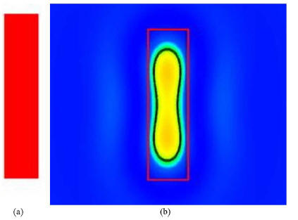
Fig. 1. Layout without OPC and its silicon image [7]. (a)
Traditional layout.
(b) Silicon image
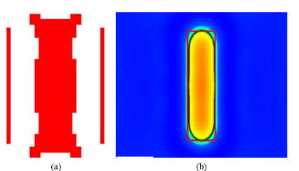
Fig. 2. Layout with OPC and its silicon image [7]. (a)
Layout with OPC.
(b) Silicon image.
phase shift mask (PSM), off axis illumination (OAI), and
sub-resolution
assist feature (SRAF), so as to overcome diffraction
limit and process imperfections. For example, mask layout for
printing the rectangle feature in Fig. 1(a) becomes Fig. 2(a) with
OPC and SRAF. As a result, the printed feature on silicon [see
Fig. 2(b)] becomes closer to the desired rectangle shape.
However, relying on RET alone is inadequate to harness the
problem because of the following reasons.
• The increasingly large gap between feature size and
wavelength
forces several aggressive RETs to be jointly applied
and thereby compounds the already complicated mask design
and increases mask cost drastically. An example in [6]
is shown in Fig. 3 to demonstrate this problem. Compared
to mask layout without OPC like Fig. 3(a), the mask layout
with OPC like Fig. 3(b) increases mask data volume, mask
writing time, and, therefore, mask cost dramatically.
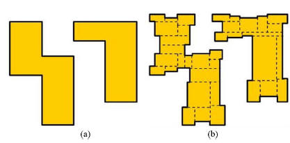
Fig. 3. OPC results in fractures in mask layout [6]. (a) Without OPC. (b)With
OPC.
• The circuit complexity keeps growing and makes RET
formidably
challenging.
• RET deployments may be obstructed or even prohibited by
an RET-unfriendly layout. Therefore, the subwavelength
printability problem has to be considered also in circuit
layout design to ensure manufacturability.
In practice, a lithography friendly and/or RET compliant
layout is often obtained through either rule based or
model-based methodology level approaches. In rule-based
approaches, lithography friendliness and/or RET compliance
are expressed as a set of recommended/hard design rules which
are applied in detailed layout design such as detailed routing
and layout compaction. This approach is fast and relatively
easy to use. However, lithography and RET procedures are so
complicated that it is very difficult to convey their requests fully
through simple rules. In model-based approaches, lithography
and RET simulations are performed on a circuit layout and any
observed problems are fed back to circuit designers for layout
modification. The model-based solutions are generally more
reliable than the rule-based solutions, but the simulations are
very time consuming and it usually takes several iterations to
reach closure.
In order to overcome the weakness of the methodology level
approaches, lithography friendliness and/or RET compliance
need to be considered directly in circuit layout algorithms. In [8]
and [9], the alternating PSM compliance is modeled as a graph
problem and layout modification algorithms are developed to
achieve alternating PSM compliance with minimum cost change
where the cost can be defined in term of area or timing. Compared
with alternating PSM compliance, the other RET procedures
are very difficult to be abstracted into concise models that
can be easily embedded in automatic layout algorithms. Recently,
the work of [7] circumvents the difficult RET abstraction
issue by optimizing interference intensity instead. This is
based on the observation that a reduced interference intensity
can alleviate the workload of RET and the interference intensity
model is relatively easier to be obtained. An OPC friendly
maze routing algorithm is proposed in [7] using the interference
intensity model. An RET aware routing algorithm based on fast
litho simulation is proposed in [10].
In layout printability optimizations, conventional design
objectives such as timing performance cannot be ignored since
timing performance heavily depends on physical layout in
today’s interconnect dominated technology [11]. In this paper,
we focus on the wire sizing problem which plays an important
role on affecting timing performance and we combine wire
sizing and spacing to improve printability of the design. There
are many previous works on wire sizing but mostly for timing
optimization alone. The work of [11] attempts to minimize
a weighted sum of sink delays for a Steiner tree. A sensitivity-
based wire sizing heuristic is reported in [12]. A dynamic
programming-based simultaneous buffer insertion and wire
sizing algorithm is proposed in [13] to achieve timing-area
tradeoff for a Steiner tree. A circuit-wise gate sizing and wire
sizing method based on local refinement is developed in [14]. In
[15], the circuit-wise simultaneous gate sizing and wire sizing
problem is solved optimally using Lagrangian relaxation. A
simultaneous wire sizing and spacing algorithm considering
coupling capacitance is introduced in [16].
We proposed a new printability model in [20]. In this
paper,
we extend that work by addressing timing optimization in addition
to subwavelength printability issues in both wire sizing and
spacing. We also show in this paper that our printability model
can be used in the aggressively optimized design to improve
printability significantly. By doing timing and printability
optimizations in series, we also imply that this approach as the
use model of the lithography optimization for interconnection
metals. Our goal is to improve wire printability, i.e., make
printed wires have sharper boundaries, so that the cost of RET
and photo-mask can be reduced. Moreover, the printability
driven wire sizing method should minimize any adverse impact
on interconnect timing performance. The major contributions
of this work are listed as follows.
• We propose a new approximated printability model for
layout optimization. The lithography procedure is so
complicated that a practical printability model becomes
a bottleneck for printability optimization. Compared to
the model in [7], our model has two advantages : 1) our
model can handle partially coherent illuminations which
is the mainstream illumination method in practical photolithography
while the model in [7] is limited to coherent
illuminations and 2) our model directly measures the
feature sharpness and considers the overall light intensity
effect instead of considering only interference light intensity
as in [7].
• The complicated printability and timing optimization
problem is solved in a two-phase approach considering
different problem natures of printability and timing. The
difficulty of the printability optimization due to its multimodal
nature is handled with a sensitivity-based heuristic.
• A coupling aware timing driven continuous wire sizing
algorithm
is also provided. The closest works are [15], which
does not consider coupling capacitance and [16], which is
only for discrete wire sizing.
Implementing litho-friendly design techniques in design
phase,
such as our approach to adjust wire sizing and spacing, will alleviate
the printability problem. It will help to reduce the effort
level of OPC/RET that has to be performed at the manufacturing
stage. This will have a direct advantage at reducing
mask cost, but the more important cost saving is realized by reducing
the number of iteration cycles of the mask correction,
which contributes to shorten the time needed to achieve volume
production. Lithographic simulation results show that our approach
can improve the wire printability in term of edge placement
error (EPE) by 20%–40% without violating timing and
wire width/spacing constraints.
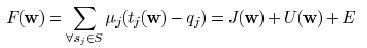
II. PROBLEM FORMULATION
The input to the wire sizing problem is a set of Steiner
trees
 representing the layout of signal nets. In
 , there is a set of wire edges
 and a set of
sink nodes  such that each edge and each sink
belong to a certain Steiner tree. Each  edge
has a width
edge
has a width
of  which is bounded in a range of
 The edge width
vector for all edges is  , location vector of
all
, location vector of
all
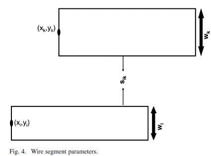
edges are  . In Fig. 4, an
example for horizontal wires is illustrated. The space between
the wires can be calculated as  .
.
Each sink  has a required arrival time (RAT)
 and a
and a
delay whose model is provided in Section IV. The printability
function  will be defined in Section III. We
will solve
will be defined in Section III. We
will solve
the following problem in this paper:
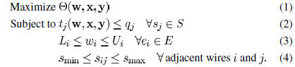
In other words, we attempt to maximize the overall
printability
of the layout subject to timing and wire width/spacing
constraints. This optimization framework can include other objectives
such as area and power consumption. We consider continuous
wire sizing as in [15] so that it is easier to handle the
complicated printability function. If discrete wire sizing solutions
are needed, they can be obtained through rounding the continuous
solutions as in [12].
The previous seemingly simple formulation is actually a
rather difficult nonlinear programming problem, since the
expressions for objective (1) and constraint (2) are complicated.
Especially, the objective function  is not
unimodal in general.
is not
unimodal in general.
Therefore, we propose to solve this problem in the following
two phases.
1) Obtain a wire sizing solution considering coupling that
satisfies constraints (2)–(4) regardless the printability.
A Lagrangian relaxation-based algorithm is described in
Section IV for solving this subproblem.
2) Based on the solution of phase 1, maximize the
printability
 while the constraints (2)–(4) are still
satisfied. A sensitivity-
while the constraints (2)–(4) are still
satisfied. A sensitivity-
based local adjustment heuristic is introduced in
Section V to solve this subproblem by adjusting both wire
width and wire spacing. The result of this phase is a much
better design in terms of printability, yet still satisfies all
the timing and wire width/spacing constraints.
The problem natures of the printability maximization and
satisfying
delay constraints are different. The delay optimizations
are net based and have no clear geometrical boundary, especially
when coupling capacitance is considered. In otherwords, the delays
for sinks far apart are mingled with each other through the
nets and coupling. In contrast, the lithographic effect from an
edge or to an edge is localized. By solving the timing constraints
first in phase 1, phase 2 can be focused on maximizing the printability
function through geometrically local adjustments. The
different problem natures also justify why our two-phase approach
is more practical than solving the entire problem using
Lagrangian relaxation as in [15]. In contrast, the problem in [15]
is unimodal as printability is not considered.
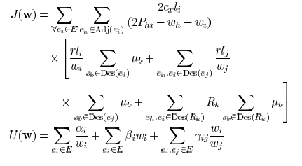
III. PRINTABILITY MODEL
A. Aerial Image
Since the printability model is based on the light
intensity
distribution on the wafer plane, we first discuss the light intensity
models for three basic types of illuminations: 1) coherent,
2) incoherent, and 3) partially coherent. In the following discussions,
we assume that the optical system is a 1* reduction
system. Although practical steppers and scanners are usually
4* or 5* reduction systems, a 1* system with the same numerical
aperture (NA) [2] gives essentially identical printing
results under the assumption of thin mask approximation and
aberration-free.
Coherent Illumination: The complex field distribution
 on the image plane (wafer) can be expressed
as
on the image plane (wafer) can be expressed
as
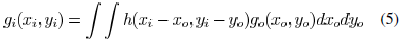
where  is the complex
field distribution on the object
is the complex
field distribution on the object
plane (mask) and  represents the impulse
response function
represents the impulse
response function
of the optical system. In the frequency domain, spatial frequency
along x and y directions are denoted as  and
and
 , respectively,
and the previous equation can be rewritten as

where  and
and
 are obtained through Fourier
transform of 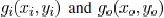 , respectively. The coherent
transfer function  is given by
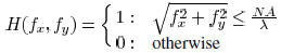
where λ is the lithographic wavelength.
Incoherent Illumination: The aerial image formation under
incoherent illumination is based on linear superposition of light
intensity
where  are
are
the light intensity distribution on the image and object planes,
respectively.
Partially Coherent Illumination: In reality, almost all
practical
photolithography systems employ partially coherent
illumination, although the coherent and incoherent illumination-
based models provide theoretic foundations for partially
coherent illumination-based models. For partially coherent
illuminations, there are several existing methods of computing
aerial image such as Abbe’s approach [19], Hopkins formula
and eigenfunction expansion [18]. Abbe’s approach and eigenfunction
expansion method decompose the illumination source
into many coherent sources, then calculates the complex fields
due to each source, and finally add together the light intensities
due to each source to obtain the total light intensity distribution.
Hopkins formula requires the computation of transmission
cross-coefficients. These existing methods are too computationally
expensive to be adopted in the wire sizing and spacing
optimization procedure.
We propose an optimization friendly approximated model for
partially coherent illuminations based on a linear combination
of coherent and incoherent imaging. In the proposed model, the
wafer image is given by

where  is the partial
coherence factor ,
is the partial
coherence factor ,  corresponds
to coherent illumination, and  approaches
incoherent
approaches
incoherent
illumination.
The complex field at one point p due to a line segment
(wire
segment) e under coherent illumination can be approximated by
a quadratic function. If the width of the segment is w, the distance
vector from the segment e to p is  then the
complex field
then the
complex field
contributed by e at p can be approximated as
 which is a quadratic function of w. The
coefficients of
which is a quadratic function of w. The
coefficients of
this quadratic function depend on the distance vector
Similarly,
the light intensity from incoherent illumination can also
be approximated as  . If there are
line segment with widths of  , and the
distances
, and the
distances
from to them are  , then the total light
intensity
, then the total light
intensity
at p is
The distance vector  is
determined differently in two cases.
is
determined differently in two cases.
If the point is around the middle of segment e as p1 in Fig. 5,
the infinite line model is applied and  is
equivalent to a distance
is
equivalent to a distance
scalar y in Fig. 5. Since the coefficient functions such as
 are multimodal and very complex, their
values
are multimodal and very complex, their
values
are saved in a lookup table. If the point is close to one end of
the segment as p2 in Fig. 5, the semi-infinite line model is employed.
In this case, the distance vector is decided
by x and
y component as shown in Fig. 5. Consequently, a 2-D lookup
table is needed for the semi-infinite line model. In contrast to
the model in [7], our model does not depend on the segment
length directly and, therefore, the number of lookup tables can
be reduced.
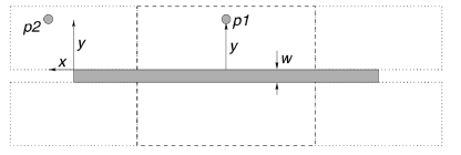
Fig. 5. Infinite line model in dashed bounding box. Semi-infinite line model in
dotted boxes.
Comparisons between the approximated model and simulation
[17] results are shown in Figs. 6 and 7 at the end of this
paper. Fig. 6 plots the contours of the amplitude of complex
field for coherent illumination with respect to the linewidth of
a feature and distance to the feature. In Fig. 7, the contours of
light intensity with respect to the linewidth and the distance are
plotted. We also pick a few real circuit patterns and compare
light intensity calculated with our approximated model and the
simulation [17] results in Fig. 8. In Fig. 8(a), we show the test
pattern we used, in Fig. 8(b), we plot light intensity result from
our models with those from SPLAT calculations. It can be seen
that the results from the approximated models are very close to
the simulation results.
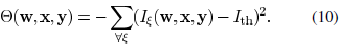
B. Printability Function
In order to print out a sharp image, we wish the overall
light
intensity inside a feature (wire segment) to be full level represented
by 1 while the light intensity outside the feature should
be 0. Ideally, there is a sharp light intensity transition along
boundary of the rectangle representing a wire segment. If the
transition threshold is denoted as  , we wish
inside segment,  outside segment. Therefore,
the ideal case is  when is on the segment
boundary. For a wire segment, we chop its boundary into
multiple small pieces which are sufficiently small, then the light
intensity on every point of a single boundary piece
 can be regarded
as the same  . Then the printability function
is defined as
. Then the printability function
is defined as
This printability model has two major differences from the
model employed in [7]. First, the model in [7] is for coherent
illumination, while ours is for partially coherent illumination
which is much closer to the practical reality. Second, the model
in [7] emphasizes on interference, while ours is focused on
image sharpness. The work of [7] attempts to limit the interference
to a target wire from its neighbor wires. However, the
effect of light from the target wire itself is not considered. In
practice, it is the overall effect of lights from the target wire and
its neighbor wire that determines the printability of the target
wire. Therefore, our model captures a more complete picture
of the printability problem.
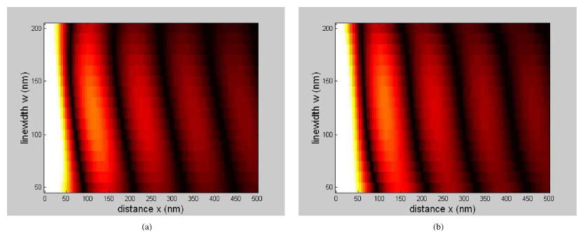
Fig. 6. Contour plot of complex field amplitude versus feature linewidth and
distance to feature for coherent illumination. (a) From lithographic simulation.
(b) From our approximated model.
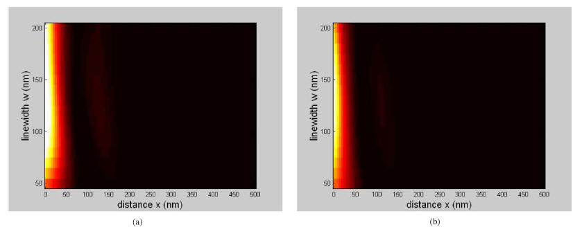
Fig. 7. Contour plot of light intensity versus feature linewidth and distance to
feature for partially coherent illumination.
(a) From lithographic simulation.
(b) From our approximated model.
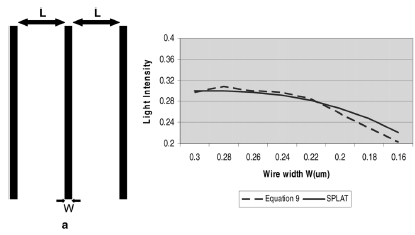
Fig. 8. Comparisons of light intensity calculations. (a) Test structure. (b)
Light intensity.
With the printability model, we are able to simplify the
complicated lithography modeling and simulations and make
it suitable for use in the design environment. In Fig. 9, we
reproduce a figure from [10] to show the relationships of light
intensity and EPE. We can see EPE is the error in x-axis
caused by light intensity error in y-axis, they are highly
correlated.
IV. TIMING DRIVEN WIRE SIZING CONSIDERING
COUPLING CAPACITANCE
In phase 1 of our method, we need to find a wire sizing
solution
which satisfies the constraints (2)–(4). Here, we perform
wire sizing without changing the center locations wires. Thus,
only w are variables and the spacing constraint (4) can be implicitly
satisfied by enforcing the width constraint (3). As in
[15], this subproblem can be solved through Lagrangian relaxation
which is formulated as
where  forms the set of
Lagrangian multipliers. Alternatively,
forms the set of
Lagrangian multipliers. Alternatively,
the problem in phase 1 can be formulated as
where  indicates the
minimum timing slack. This minimum
indicates the
minimum timing slack. This minimum
slack maximization problem can also be solved through
Lagrangian relaxation as
Fig. 9. Light Intensity and EPE.
We can see that the Lagrangian problems (11) and (12) are
very similar with each other and can be solved in a similar
method. The value of the Lagrangian multipliers can be found
using the subgradient method as in [15]. For each set of fixed
Lagrangian multipliers, the problem (11) is equivalent to minimizing
a weighted sum of sink delays [16]. However, the algorithm
of [16] is for discrete wire sizing and the work of [15] does
not consider coupling capacitance. Therefore, we introduce a
continuous wire sizing algorithm considering coupling capacitance
as follows.
First, we describe the expression of delay function
 for
for
a sink  . For an edge
 its length is
 and its width is
 . Its edge capacitance is
 and its downstream capacitance
is  . The wire resistance coefficient is
denoted as r. Consider
. The wire resistance coefficient is
denoted as r. Consider
a sink node  in a Steiner tree
 with source node at
 ,
,
driver resistance  , and total load
capacitance
, and total load
capacitance  . Then,
the delay  to sink
 can be expressed as
The area, fringing, and coupling capacitance coefficient
are represented
as  , and
, and  ,
respectively. The set of edges adjacent
,
respectively. The set of edges adjacent
with  is denoted as
 . The wire pitch between two
edges  and
is
and
is  . Then, the edge capacitance
 can be
obtained as
The objective function (11) can be decomposed as
where E is a constant. Function
 is the coupling related
part and  is similar as the delay function in
[15] where
is similar as the delay function in
[15] where
coupling capacitance is not considered. They can be expressed
as
where  indicates the
set of descendant edges of
indicates the
set of descendant edges of 
and  are positive constants.
According to [21], is
a unary posynomial and, therefore,
can be optimized through convex programming. In order
to optimize  , the convexity of
needs to be investigated
, the convexity of
needs to be investigated
as well.
Theorem 1: Function is
convex.
Proof: It can be observed that
is a positively linear
combination of the following base functions:
where D is a positive constant and

 . Therefore,
is convex if all of the previous base
. Therefore,
is convex if all of the previous base
functions are convex.
Fig. 10. Illustration on relative positions among nodes and edges.
Let  and
and
 , then the Hessian
matrix for  can be derived as
For an arbitrary vector
 , we can obtain

Hence,  is a convex
function. Similarly, it is straightforward
is a convex
function. Similarly, it is straightforward
to show that 
are also convex functions.
Since is convex and
is a posynomial, there is a
unique global minimum solution for [21].
Therefore, the
global minimum solution can be reached through iterative local
optimization as in [21]. In each local optimization, wire sizing
is performed for only one edge  while the
widths of the other
while the
widths of the other
edges are fixed. We use  to denote that edge
 and sink
 are in the same Steiner tree. Thus, the
delay function
are in the same Steiner tree. Thus, the
delay function
in the local optimization becomes
where  and
and
 are positive constants. In the previous
equation, the first term represents the impact of wire resistance
of  on its descendant nodes. For example, the
effect of
on its descendant nodes. For example, the
effect of  on
on
sink 1 and sink 2 in Fig. 10. The second term reflects the effect
of wire self capacitance on sink nodes in
the same tree, as
 for sink 1, 2, and 3 in Fig. 10. The third
term represents
for sink 1, 2, and 3 in Fig. 10. The third
term represents
the product of wire resistance of and
coupling capacitance
of and the effect on its descendant nodes.
For the example in
Fig. 10, the wire resistance of and its
coupling capacitance
with  affect the delay at sink 1 and 2. The
last term shows that
affect the delay at sink 1 and 2. The
last term shows that
the coupling capacitance due to wire
presents a capacitive
load to its Steiner tree and the Steiner tree it is coupled with.
For example, the width of edge  affects the
delay of sink 1, 2,
affects the
delay of sink 1, 2,
and 3 in Fig. 10. Fig. 10 also shows that a wire segment could
be part of the Steiner tree edge. Here, we define the portion of
the Steiner tree as a wire segment if the coupling remains the
same across the whole segment. For example,
is a segment,
but the rest of the wire toward sink 1 is another segment. This
way, we are much more flexible for optimization since a single
physical wire can have different width across it.
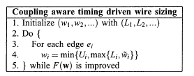
Fig. 11. Timing driven wire sizing algorithm.
Lemma 1: Function  is
convex.
is
convex.
Proof: It can be shown that
If there is value  satisfying ,
then  has a unique minimum solution at

 . Please note that
 is
is
a fourth-order equation which has closed-form solutions. Based
on this local optimization, the algorithm of minimizing
subject to wire width constraints is shown in Fig. 11.
Theorem 2: The timing driven wire sizing algorithm can
converge
to the optimal solution and the complexity of the algorithm
is  , with n being the number of wire
segments.
, with n being the number of wire
segments.
Proof: The proof is similar as the proof of Lemmas 2 and
3 in [21], and is omitted here.
V. PRINTABILITY OPTIMIZATION
The feasible solution obtained in phase 1 is fed to phase
2
in which the printability  is maximized by
adjusting
is maximized by
adjusting
wire width and spacing. The feasibility in terms of (2)–(4) is
maintained, which ensures that there is no violation on timing
and wire width/spacing rules.
Equations (9) and (10), indicate that the printability
function
is an eighth-order polynomial in general , although this is an approximated
model. We employ a sensitivity-based heuristic similar
as in [12] to solve this complicated problem. The sensitivity
of the printability function for a certain wire can be obtained
as
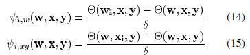
where  is the
sensitivity with respect to the wire width
is the
sensitivity with respect to the wire width
 is the sensitivity with respect to the
center location
is the sensitivity with respect to the
center location
of the wire. Here, we use vertical wires as an
example,
 . Horizontal wire segments
can be handled in a similar way. By changing wire width and
center location of the wire, we adjust both the width of the wire
and space of the wire to its neighboring wires to improve the
printability function while the wire size and spacing rules are
satisfied. Also, we do incremental timing analysis to make sure
the required arrival time stays accurate.
Even though the printability function
 is based
on the light intensity of every wire segment in the entire
layout, the computation of the sensitivity  and
and
 can be limited to a geometrically local
region.
can be limited to a geometrically local
region.
This is because a change on wire width or wire space affects
light intensity of only a local region close to that wire segment.
Usually, the effect of a change decays to negligible level at
a location more than  is the lithographic
wavelength)
is the lithographic
wavelength)
away from the location of the change. Hence, we generate a
window by expanding the wire segment i by  on
each of its
on
each of its
four sides. The computation of sensitivity  and
and
 can be limited within this window. After the
sensitivity for every wire is obtained, the wire with the maximal
value of 
is selected to be changed. The pseudo code of the printability
optimization is outlined in Fig. 12.
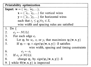
Fig. 12. Printability optimization heuristic.
When we attempt to tune the width or center location of a
wire, the constraints on wire size and wire spacing are enforced.
In addition, we need to ensure that there is no timing violations
due to this change. Even though there is analytical formula
for sink delay  of a sink
 with respect to edge
 , the delay constraint function sometimes is
equivalent to
, the delay constraint function sometimes is
equivalent to
a third-order polynomial of  and the
resultant feasible range
and the
resultant feasible range
for  is not necessarily continuous.
Therefore, we just check
is not necessarily continuous.
Therefore, we just check
the timing feasibility of each change instead of finding an analytical
bound for a change. If a change of wire width and/or
space causes any delay constraint violation, this change is forbidden.
The pseudo code for the sensitivity-based heuristic is
shown in Fig. 12. We change every wire segment at most once
during the optimization. After each change, we need to update
the timing for the path that contains this target segment, as well
as timing of the paths that contain any wire segment that couples
into the target segment. Let P be the maximum number of wire
segments that couples into any given wire segment in the design,
G be the maximum number of wire segments in any given
timing paths in the design, the complexity for printability optimization
is  . Typical value of P would be 2 as we
only consider closest neighboring wire segment of the target
segment. Also, G is typically much less than the total number
of wire segment n.
VI. EXPERIMENTAL RESULTS
Our method is implemented in C++ and the experiment is
performed on a SUN Sparc Ultra-80 workstation with four
450 MHz CPU and 4 GB RAM. Table I shows the number of
nets, horizontal wires, and vertical wires for the benchmark
circuits. Based on 90-nm technology, the wire width is allowed
in a range between 100 and 300 nm, while the wire pitch
is 400 nm. The light intensity threshold  at
wire segment
at
wire segment
boundary is chosen as 0.3, since this is usually where light
intensity slope is the greatest. Here, light intensity is relative
intensity. Light intensity at the wafer when there is no mask
between light source and the wafer is defined as 1.
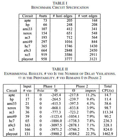
Since there is no previous work on this timing and
printability
optimization problem, we list the results of the two phases of our
method in Table II. The number of sinks with timing violations
for each case is in column 2. After phase 1, all timing violations
are eliminated as indicated in column 3. The printability
function  values after phase 1 are shown in
column 4. The
values after phase 1 are shown in
column 4. The
printability after phase 2 and the percentage improvement are
in column 5 and column 6, respectively. It can be seen that our
sensitivity-based heuristic can yield 4%–22% improvement on
the printability function  without timing
violation. Meanwhile,
without timing
violation. Meanwhile,
all wire width/spacing rules are also satisfied. The runtime information
is shown in the right-most column. This computation
speed is reasonable for practical applications.
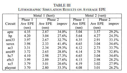
In order to validate our approach with a precise model,
lithographic
simulation [17] is performed on the layout result of
Phase 1 and Phase 2. SPLAT is a simulation program to model
projection printed images using a 2-D optical image. Developed
at UC Berkeley, it is one of the first tools in this field. One of the
most important and obvious metric for design printability is the
average EPE [10]. EPE is the distance between a printed edge
to the location where this edge is intended to be in the design.
Smaller EPE means that the printed edge is closer to its intended
location. Designs with smaller EPE will be easier for OPC/RET
in the manufacturing stage to further reduce EPE to spec. We
compare the average EPE for the designs before and after printability
optimization. The simulations for wires on Metal 1 and
Metal 2 are conducted separately and the results are summarized
in Table III. These data show that our method can improve the
average EPE by about 20%–40%. Considering that no OPC has
been applied yet, such improvement is quite significant.
VII. CONCLUSION
Lithography friendly design is a concept that aims to
reduce
litho process complexity so that volume production of the design
can be achieved faster in the laboratory while reducing mask
cost. In this paper, we propose an approach that adjusts wire
size and space to optimize layout printability while maintaining
design performance. A new printability model is proposed to
handle partially coherent illuminations. The complicated printability
optimization problem is solved in a two-phase heuristic.
A coupling aware timing driven continuous wire sizing algorithm
is also introduced. Experimental results from lithographic
simulations confirm the effectiveness of our method.
| Prev | Next |